PCB Fab and Assembly -- http://www.bittele.com/ -- PCB Fab and Assembly
Showing posts with label altium designer. Show all posts

Monday, June 11, 2012

Best Practices in Printed Circuit Board Design (Part 2)


Part Research and Selection

The most fundamental building part of a design is the physical component (such as resistors, operational amplifiers, transistors and digital components). Part research and selection requires the evaluation of components to investigate how each will work as a part of a design topology.
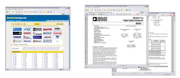
Information on device performance can be found at a number of online resources that housedatasheets. The datasheet contains information such as operating points, switching characteristics, design considerations etc…
Some web-sites where datasheets can be found include (but are not limited to):
  1. DatsheetCatalog.com
  2. Analog Devices Inc.
  3. Texas Instruments
  4. ON Semiconductor
Most component manufacturers also have datasheets available on their web-site.

Figure 3 - Example of datasheets
Many engineers like to gain a better understanding of how a component operates to complement the information on a datasheet. The first, time consuming method is to purchase the various components and physically breadboard a prototype to interrogate and analyze the device.  This can require purchasing multiple devices and breadboarding at the most preliminary stages of the design process.
The second and more advantageous method begins to integrate the fragmented nature of the traditional PCB design flow. A capture and simulation environment can be used to select a device and simulate its overall behavior. Performance can be evaluated without needing to purchase and physically breadboard.
For example, in NI Multisim parts can be selected from a database of components, each of which has a simulation model associated with it to visualize operation. In the capture and simulation environment a design can be quickly built and simulated to view the overall operation of a device. The fact that no breadboards are required means a shortened component selection process.


Best Practices in Printed Circuit Board Design (Part 1)


Overview


The manner in which electronics as consumer devices and industrial machinery has become an integral part of our daily lives needs little introduction or description. From complex machinery in factories, to computers, engineers have transitioned their ideas to conception of such devices through various technology including small rugged, inexpensive and reliable printed circuit boards (PCBs).

The design engineer faces a number of hurdles in the design of such devices, most notably the fact that traditionally each stage in their design flow is segregated, between part-selection, design, and validation.

National Instruments provides a complete PCB design platform with the ease-of-use and power of NI Multisim capture and simulation, and the integrated NI Ultiboard layout and routing environment. Built upon a platform which simplifies the board-level simulation process with intuitive SPICE analyses and an expandable measurement interface, the complete PCB solution from NI also provides the unique capability of integrating the PCB design flow with real measurements.

As we will explore through this article, it is the unification between design and measurements (a concept known as integrated design and test) which provides the basis of for better addressing the hurdles in the design, verification and production of printed circuit boards.

This article is an overview of the design flow and the Best Practices in using the features of NI Multisim, NI Ultiboard and NI LabVIEW to transition from schematic, simulation, layout to manufacturing.

Introduction

In the PCB design flow, engineer encounters a number of steps which are ever present. These steps are common to the design, validation and fabrication of all PCBs, around the world.
In analyzing the overall PCB design flow it becomes apparent that the major productivity gap is the lack of integration between each of these design steps. The laborious task of transferring data, reproducing work, and being unable to effectively leverage previous data adds time and inefficiency to the creation of circuits.
One may ask what are these steps in the design flow, and how does the lack of integration impact the engineer? Let us look at the traditional flow in Figure 1 below.

Figure 1 - The Traditional Design Flow

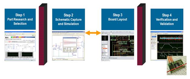
There are effectively four stages during the PCB design flow:
  1. Part Research and Selection
  2. Schematic Capture and Simulation
  3. Board Layout
  4. Verification and Validation
The brick walls in figure 1 represents isolated stages in the traditional design flow. This isolation means that through the PCB design flow different applications must be used, or data needs to be manually manipulated for the next stage.
Traditionally step 2 (schematic capture and simulation) and step 3 (board layout) are integrated, usually as a part of a single corporate tool-chain. However, every PCB design flow begins with part research, and ends with prototype validation. Both stages are separate and isolated from these core design steps. This becomes of concern for many engineers because there is inherently a large degree of iteration throughout the design of a PCB. The lack of integration means that this "iterative design" becomes more difficult and time consuming. The goal is therefore to remove those “brick walls” of isolation and to integrate the PCB design flow, by connecting part research with the design and prototype validation stages (as seen in the figure 2 below).


Figure 2 - An Integrated Design Flow

In this article, we will investigate a design procedure that is integrated as in figure 2 above. As you will soon see it is through the type of design flow that integrates traditionally fragmented steps, that a foundation of best practices is developed.


PCB Design Flow

The PCB design flow consists of four distinct stages. There is the part research and selection stage, schematic capture and simulation, board layout, and finally board verification.


Figure 2 - The PCB Design Flow

If you are unfamiliar with any of these stages, I recommend that you view the following page, that will be able to provide you additional details on each stage, and how best to handle design: Best Practices in PCB Design.
The remainder of this page will talk about board layout and design. Prior to this layout stage, you must first define a schematic capture (or circuit diagram) in a tool such as NI Multisim. A schematic capture tool allows you to place symbols for electronic components and wire them together. Each of these symbols (for the amplifier, resistor etc…) are linked to a symbol that represents the dimensions and shape of an actual device used on a PCB. So a resistor symbol is associated with a real-world resistor footprint or landpattern. This landpattern is what we use on our board layout in order to define our final PCB.

Figure 3 - Schematic Capture


You must transfer a schematic to a board layout application (such as NI Ultiboard). From here you define the board outline (form factor), place parts onto the board surface (landpattern placement) and route copper connections (make pathways for signals to be conducted through the PCB).

Figure 4 - Board Layout

After these stages, you can export your design to an industry standard format (Gerber) from which a physical board is fabricated. The rest of this page will speak to this physical hardware, and what it consists of.

Introduction to PCB Design


A Printed Circuit Board (PCB) is a rugged, copper and non-conductive substrate based structure to connect electrical components (for example the green board inside a common electrical appliance is a PCB). The PCB is the backbone of electrical devices, allowing you to connect passive (resistor, inductor, capacitors etc…), active (operational amplifiers etc…) and embedded devices together, into specific form factors to fit the design need. Connections between the components are made through copper connections (routes) which become passageways for electrical signals.
PCBs were first developed by an Austrian Engineer named Paul Eisler. Born in Vienna, and educated at the Vienna University, he made his way to the United Kingdom in the 1936. He began developing the circuit manufacturing process during the Second World War where he earned a number of patents dealing with the etching process, to define the various routes and electrical conduits on your board.

Figure 1 - PCB Example