
Overview
The manner in which electronics as consumer devices and industrial machinery has become an integral part of our daily lives needs little introduction or description. From complex machinery in factories, to computers, engineers have transitioned their ideas to conception of such devices through various technology including small rugged, inexpensive and reliable printed circuit boards (PCBs).
The design engineer faces a number of hurdles in the design of such devices, most notably the fact that traditionally each stage in their design flow is segregated, between part-selection, design, and validation.
National Instruments provides a complete PCB design platform with the ease-of-use and power of NI Multisim capture and simulation, and the integrated NI Ultiboard layout and routing environment. Built upon a platform which simplifies the board-level simulation process with intuitive SPICE analyses and an expandable measurement interface, the complete PCB solution from NI also provides the unique capability of integrating the PCB design flow with real measurements.
As we will explore through this article, it is the unification between design and measurements (a concept known as integrated design and test) which provides the basis of for better addressing the hurdles in the design, verification and production of printed circuit boards.
This article is an overview of the design flow and the Best Practices in using the features of NI Multisim, NI Ultiboard and NI LabVIEW to transition from schematic, simulation, layout to manufacturing.
Introduction
In the PCB design flow, engineer encounters a number of steps which are ever present. These steps are common to the design, validation and fabrication of all PCBs, around the world.
In analyzing the overall PCB design flow it becomes apparent that the major productivity gap is the lack of integration between each of these design steps. The laborious task of transferring data, reproducing work, and being unable to effectively leverage previous data adds time and inefficiency to the creation of circuits.
One may ask what are these steps in the design flow, and how does the lack of integration impact the engineer? Let us look at the traditional flow in Figure 1 below.
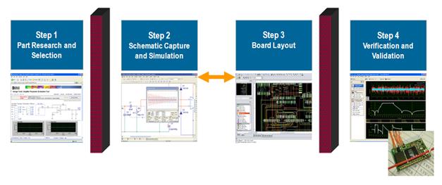
Figure 1 - The Traditional Design Flow
There are effectively four stages during the PCB design flow:
- Part Research and Selection
- Schematic Capture and Simulation
- Board Layout
- Verification and Validation
The brick walls in figure 1 represents isolated stages in the traditional design flow. This isolation means that through the PCB design flow different applications must be used, or data needs to be manually manipulated for the next stage.
Traditionally step 2 (schematic capture and simulation) and step 3 (board layout) are integrated, usually as a part of a single corporate tool-chain. However, every PCB design flow begins with part research, and ends with prototype validation. Both stages are separate and isolated from these core design steps. This becomes of concern for many engineers because there is inherently a large degree of iteration throughout the design of a PCB. The lack of integration means that this "iterative design" becomes more difficult and time consuming. The goal is therefore to remove those “brick walls” of isolation and to integrate the PCB design flow, by connecting part research with the design and prototype validation stages (as seen in the figure 2 below).

Figure 2 - An Integrated Design Flow
In this article, we will investigate a design procedure that is integrated as in figure 2 above. As you will soon see it is through the type of design flow that integrates traditionally fragmented steps, that a foundation of best practices is developed.


No comments:
Post a Comment
Note: Only a member of this blog may post a comment.